
Jywsoft
- No matter how many PCBs I design, I always find myself constantly reviewing the network paths on the schematic layer and keeping track of the routes on the PCB. The complexity reminds me of a maze where only one path is correct for a particular network. It is imperative that all connections are correct as mistakes made here will come back to haunt you later in the form of a redesign.
- The best way to ensure network accuracy is to isolate the network so that each connection can be visually verified and edited, if needed. Without a powerful software design tool, creating and editing schematic data and PCB footprint can be quite difficult and time consuming. On the other hand, with the right PCB design software, functions and capabilities, the design process can be greatly simplified and the time required to create design files is greatly reduced.
- Altium Designer® is a powerful unified design environment for creating schematics and PCBs. This package is designed to simplify functional data-heavy tasks, so the main part of the process is the creative side, which lies with each individual designer. One of the capabilities that facilitate this for the designer is the ability to isolate and evaluate individual networks for accuracy. Highlighting the grid will help you simplify your schematic and PCB design. In Altium Designer, there are many options that allow you to take advantage of this capability to simplify the verification of connections and circuit paths and ensure that the design you submit to the manufacturer accurately reflects the printed circuit board that you are using. you need to build.
Highlight Nets to simplify schematic design
- Although the schematic does not provide the layout that will be present on your production board, it is essential that it is accurate and complete. In all but very limited cases, such as when you're adding a pad or an addition to a previous design, or if the layout is fairly simple, your PCB design will usually start Start by creating a new schema. Here you can define all the elements and create your grid, as shown in the diagram below.
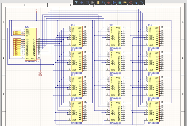
Diagram example without grid is highlighted
- The connections in the diagram are all easily visible in normal viewing, but the situation is quite complex and the connections between the buffer and decoder are difficult to trace due to overlap between the meshes. Altium Designer includes a feature that allows you to view, select, or zoom into a specific network in the diagram. Selecting or marking a grid allows you to keep the entire network in a magnified view.
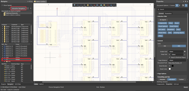
- To select specific grids, open the Navigation panel while you have the diagram open. If you click the “Interactive Routing” button (outlined in the red box in the image below) at the top of the panel, you will see the pointer change, allowing you to select a specific connection in the diagram. his stuff. As soon as you click on one of the wires, the entire wire will be selected and the rest of the diagram will become semi-transparent. This will also enlarge the portion of the diagram containing the network so that it fills the entire window.
Example diagram with a marked network
- In another case, you might know the name of the network you want to test, but you're not sure where exactly it appears in the diagram. In this case, you can find the specific network in your diagram by browsing the "Network/Bus" list in the Navigation panel. When you click on one of the grids in the list, it will highlight in the same way as shown above.
- Finally, let's say you want to automatically select all the wires in the network. In this case, you'll want to use the "Network/Bus" list in the Navigation panel. Right click somewhere in the “Network/Bus” list and you will see a drop-down menu with the option “Select Audience”. When you enable this feature, you can click through the list of grids and all connections related to this network will be automatically selected. This allows you to modify or delete and the entire network in your diagram without having to keep track of each part of the network and select individual parts.
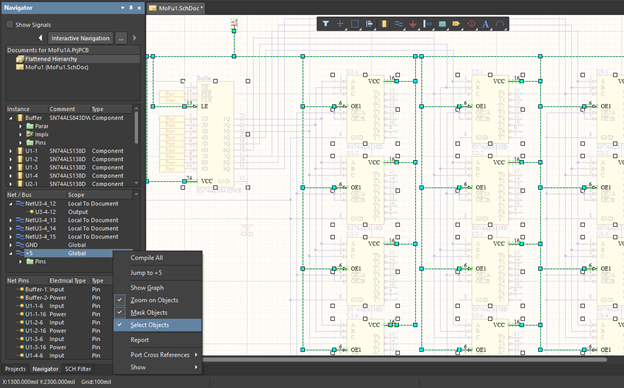
Diagram example with a selected network
- Note that this feature is useful if you come across a design that is updated many times and becomes too complicated. As you begin your design, you can avoid the kind of complexity that involves multiple crossing wires in a diagram when you create your design by using a hierarchical diagram. This allows you to define connections between diagrams and avoid the kind of confusion shown above. However, you can always access this network's elevation alignment feature to highlight, select, or simply zoom into each individual grid.
Mark Nets in PCB Editor
- Today, most PCBs consist of components packed densely in a small area. More often than not, these boards contain SMD and multiple signal layers, as shown in the example below. It is almost impossible to accurately trace any trace to this layout without help. Fortunately, Altium Designer provides help in the form of the ability to highlight meshes, even if they extend to multiple layers.
- For example, see the MiniPC - SODIMM project in the Examples folder, provided in your library when you installed Altium Designer. If you open this project and open the PcbDoc file, you will see a complex layout for the computer memory module. The image below shows this table with all layers enabled and visible. If you want to convert which layer is displayed, you can click the “LS” tab at the bottom left of the PCB Editor window to open the View Configuration dialog.
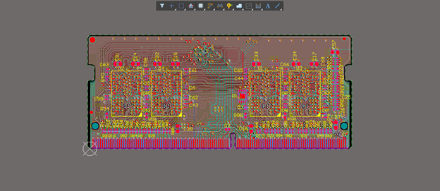
Example of PCB with all layers visible and no grid marked
- To highlight specific grids, click the Panels tab at the bottom right of the PCB Editor and open the PCB board. This panel will list all the net layers and the meshes included in each layer. The image below shows the SODIMM board with the negative end of the CLK net layer highlighted; This network is named CL0_N.
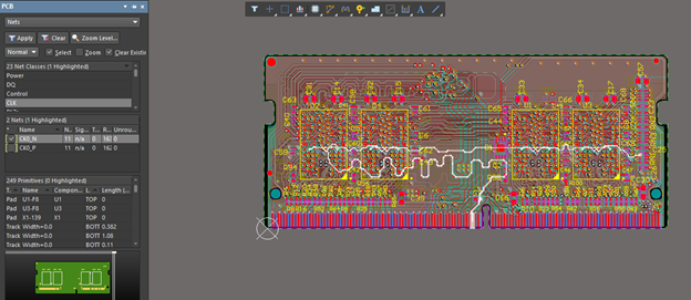
Example of PCB with CLK net layer and CL0_N network marked
- This panel also allows you to zoom into the selected signal network if you want, and you can toggle the zoom function at the top of the PCB board. Note that this option has been disabled in the image above. You can also change the color of each part of the table and the color of the highlighted grid in the view configuration manager. Scroll to the bottom of View Configuration Manager and expand the System Colors menu. This allows you to modify the color scheme in the PCB Editor, as well as the color of the selected/marked network. The example is shown below, where the CL0_N network is purple.
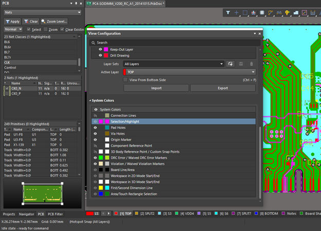
Modify the color of the highlighted grid in the View Configuration Manager
Third option: Board Insight screen
- Instead of going through the Table tab, you have the option to highlight the grids by hovering over them. This option can be set using the Board Insight Display, which can be accessed from the Preferences menu in the PCB Editor preferences. With this set of options, you can quickly switch from network connection to verification network just by moving the mouse.
- Making sure that your printed circuit board design, schematic and board layout are connected correctly is crucial to the successful fabrication and assembly of your PCB project layout. Sending your design out with incorrectly routed or misconnected meshes will be detrimental to your product development. Extended turnaround times and additional costs are two of the penalties you may face. These can be avoided by using grid marking capabilities.
- Altium Designer is a powerful software package with advanced features and schematic and PCB creation can be simple and easy. The program's unified design environment and extensive functionality provide you with many tools to simplify your design experience and free you from design problems. The PDNA package, for example, allows you to check power integrity across the entire signal grid and power/ground plane during the design process. If changes are needed, they can easily be applied to both your schematic and PCB. Highlighting grids in your schematics and PCBs helps you make design changes quickly and easily.
- For more information on how to highlight grids for your schematic and PCB designs, contact Altium Designer's PCB design specialist.
